Description
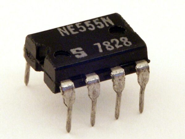
1 GND Ground reference voltage, low level (0 V)
2 TRIG The OUT pin goes high and a timing interval starts when this input falls below 1/2 of CTRL voltage (which is typically 1/3 VCC, CTRL being 2/3 VCC by default if CTRL is left open). More simply we can say that OUT will be high as long as the trigger is kept at low voltage. Output of the timer totally depends upon the amplitude of the external trigger voltage applied to this pin.
3 OUT This output is driven to approximately 1.7 V below +VCC, or to GND.
4 RESET A timing interval may be reset by driving this input to GND, but the timing does not begin again until RESET rises above approximately 0.7 volts. Overrides TRIG which overrides THR.
5 CTRL Provides “control” access to the internal voltage divider (by default, 2/3 VCC).
6 THR The timing (OUT high) interval ends when the voltage at THR (“threshold”) is greater than that at CTRL (2/3 VCC if CTRL is open).
7 DIS Open collector output which may discharge a capacitor between intervals. In phase with output.
8 VCC Positive supply voltage, which is usually between 3 and 15 V depending on the variation.
Pin 5 is also sometimes called the CONTROL VOLTAGE pin. By applying a voltage to the CONTROL VOLTAGE input one can alter the timing characteristics of the device. In most applications, the CONTROL VOLTAGE input is not used. It is usual to connect a 10 nF capacitor between pin 5 and 0 V to prevent interference. The CONTROL VOLTAGE input can be used to build an astable multivibrator with a frequency-modulated output.


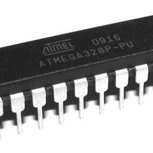 atmega328p with bootloader
Reviews
There are no reviews yet.